VACS:Projects:Hardware:LPS
Contents |
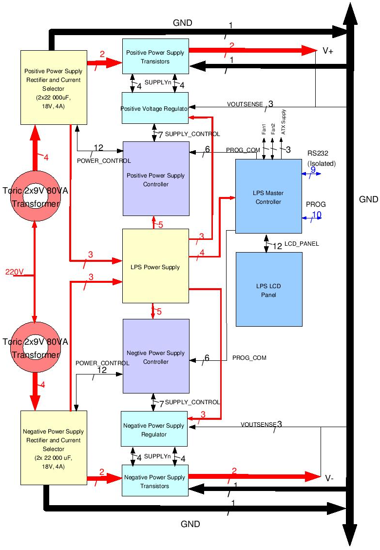
Architecture Overview
- red lines indicate hot points
- black lines indicate the ground, signal or control lines
- blue lines indicate external connection (remote control and programming)
- strong line will draw more current
Transformers
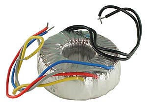
Two toric transformers are used: one for the positive voltage and one for the negative voltage. This choice was motivated by:- the low profile of these transformers
- the need for at least 4x9V supply to optimize the 4 output supplies while reducing the total heat dissipation (for low voltage outputs)
- the room available in the final LPS case
Each transformer will deliver 80VA on 2x9V. This represents a maximum current arround 4.4A. The toric transformer used for positive voltage is also used for the power supply of LPS itself. This means that it is possible to use a single toric transformer but LPS will only deliver positive voltage.
LPS Power Supply
The power supply controllers and the master power supply board need themselves a power supply. A positive power supply controller uses the following supplies:
- +24V, -5V
- A power supply controller contains operational amplifiers to drive the output power supply transistor. The +24V and -5V was chosen so that the outputs of the operational amplifiers will have a full range of 0 to more than 18V. The AOP that is used is a TL074 whose maximum supply voltage is 36V.
- +5V
- The ATmega8 and other control logic power supply.
The negative power supply controller will use a different voltage for the operational amplifiers. A +5V and -24V is used so that the outputs can follow the required voltage to drive the power supply transistors.
To obtain the LPS power supplies we use the toric transformer of the positive power supply. The +24V and -24V are obtained by a voltage multiplier from the 2x9V toric transformers. In theory it can reach 36V so the decoupling capacitor is chosen to support at least 50V.
Rectifiers
The rectifier board contains the diodes to convert the alternating current into direct current. Four diodes are used to convert the 2x9V into two positive unregulated outputs. The diodes form a bridge rectifier connected to the 2x9V transformer outputs which are in serial.
Two 22000uF capacitors are present on each output to produce a steady DC. The DC outputs may vary between 11V and 13V due to the toric transformer. Indeed the toric transformer has an output that could be 10% higher without any load.
<math> 18 \times \sqrt{2} - 1.4V = 24V </math>
11.7V .. 12.9V 23.4V .. 25.7V
Under a maximum load of 3A (thus overloading the transformer) the output voltage swing will be arround 2.7V for the 25V output and 1.3V for the 12V output (at 100Hz).
<math> dV = \frac{I \times 0.007}{C} </math>
Positive Power Supply Controller Board
The Power Supply Controller Board controls two power supplies. One is a fixed voltage and the other is variable.
Fixed Power Supply
This power supply has a fixed output voltage that is adjusted by a small trimmer at the rear of LPS. The trimmer will not allow a full range of output voltage. This power supply is either connected to the 11V unregulated supply or to the 22V supply. In the first case, it will allow a fixed power supply in the range 0..9V and in the second case a fixed power supply in the range 9..20V.
Variable Power Supply
The variable power supply allows a full voltage range of 0 to 20V. The voltage is controlled by a 8-bit DAC that controls a current between 0 and 2mA. That current is sinked from a resistor that is connected to the output voltage. The higher the current the higher the output voltage. The resistor value is chosen with the following formulae: <math> R = \frac{Vmax}{2mA}
Vmax = 20V => R = 10K </math>
The current reference is created from the 2.5V reference voltage. The DAC resistor is chosen with the following formulae: <math> R = \frac{Vref}{Iref} </math> Vref = 2.5V, Iref = 2mA => R = 1250
Measuring the current
To measure the output current a resistor is used in the path of the power transistor controlling the output voltage. In fact the resistor is composed of two parallel networks composed of a resistor followed by a high power MOSFET transistor. Each MOSFET transistor can be switched on or off. When both are off, the corresponding output voltage is switched off. This feature is used by the protection system controlled by the power supply controller. To compute the current we just need to measure the voltage of the resistor. We must take into account the Rdson of each MOSFET because they are in the current path. The IRF9540 has an Rdson arround 0.117 ohm and some others have an Rdson that can reach 0.48 ohm. In that later case it is possible to remove the resistor to only have two parallel MOSFETs. The table gives the different values of R1 when at least one MOSFET is on.
| R1 | Rdson max | I max | V max (Rdson = 0) | V max (Rdson max) |
|---|---|---|---|---|
| 0.66 (3W) | 0.117 | 2.13A | 1.4V | 1.65V |
| 0.22 (3W) | 0.117 | 3.69A | 0.81V | 1.24V |
| 0.165 | 0.117 | 4.90A/5.28A | 0.81V | 1.24V |
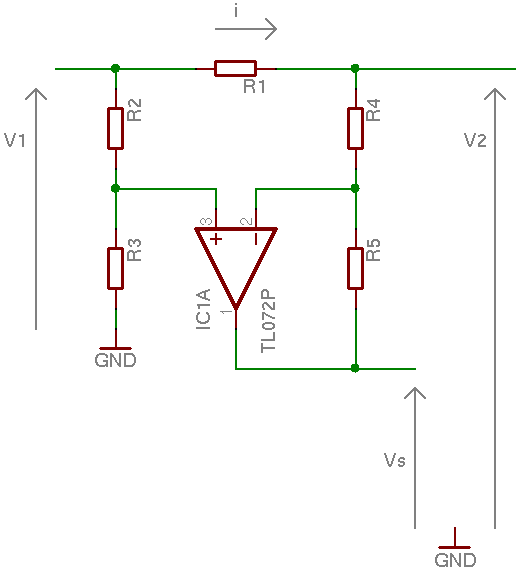
Two ways can be used to measure the current or voltage arround R1.
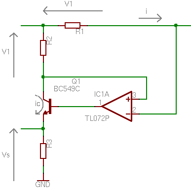
The current is measured with an operational amplifier. The output current i creates a voltage drop in the resistor R1 that is used to measure the output current. The operational amplifier drives the transistor Q1 to maintain the same voltage drop on resistor R2. The current ic which flows in R2 is therefore proportional to the output current i. The current ic goes in R3 and creates a voltage which depends on i. The voltage on R3 is defined by the formula:
      R3 * R1
Vs = --------- * i
         R2
The operational amplifier has its inputs which can range from 0 to the maximum output voltage supported by the power supply. Therefore we must provide it a power supply that is 1 or 2 volts greater than the maximum output voltage.
A second issue more important occurs when the output power supply has a low voltage and high output current. We have a constraint that Vs < Vo. If this is not satisfied, then the transistor Q1 cannot drive the current in R3 from its collector. Due to the NPN transistor, the current that flows in R3 will come from the Q1 base and Vs will grow without any relation to the current i.
| R1 | R2 | R3 | i | Vs |
|---|---|---|---|---|
| 0.66 | 2.2K | 15K | 1.2A | 5V |
| 0.165 | 2.2K | 15K | 4.8A | 5.4V |
       R3 * R1
  Vs = -------- * i
          R2
The gain created by R3/R2 is chosen to be near 4 to maximize the output voltage swing for the analog converter.
One advantage of the differential solution is that we do not have the limitation or constraint on the output voltage. It also offers a low impedance result due to the operational amplifier output.


