VACS:Projects:Hardware:LPS:RegulatorBoard
From VACS
(Difference between revisions)
(→Output Load) |
|||
| Line 1: | Line 1: | ||
==Output Load== | ==Output Load== | ||
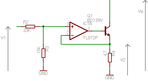
| − | [[Image:lps_output_load_study.png|thumb|256px|left|Output Loads]] The output load is intended to create a variable resistive charge on the outputs. This charge is used to dump the output capacitors. | + | [[Image:lps_output_load_study.png|thumb|256px|left|Output Loads]] The output load is intended to create a variable resistive charge on the outputs. This charge is used to dump the output capacitors. The variable resistive charge is composed of a small power resistor and a medium power transistor that drives the current on the resistor. The operational amplifier maintains arround the resistor a voltage V2 that represents a fraction of the voltage V1 (0.3125). The input voltage V1 is in the range 0..5V and the voltage V2 is in the range 0..1.56V. |
