VACS:Projects:Hardware:LPS:RegulatorBoard
From VACS
(Difference between revisions)
| Line 1: | Line 1: | ||
| − | ==Output Current Protection== | + | ==Description== |
| + | The power supply regulator is responsible for regulating the voltage of the output power supply. It is composed of two boards, one that integrates the voltage regulator for 2 power supplies and another board that contains the output power transistor and last stage filter. | ||
| + | |||
| + | ===Output Current Protection=== | ||
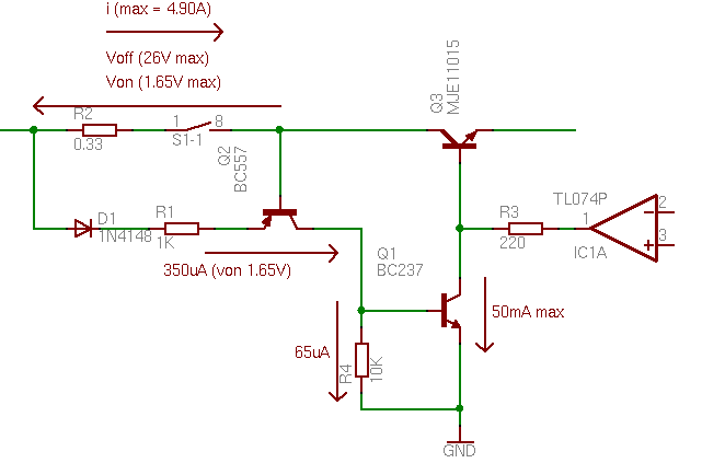
[[Image:lps_output_current_protection_study.png|thumb|384px|left|Output Current Protection]]The system has in fact two output current protections. One in the [[VACS:Projects:Hardware:LPS:ControllerBoard|power supplt controller board]] and another one in the voltage regulator board. The first protection has an impact on the voltage reference that drives the regulator board. The second protection is more traditional. A resistor R2 combined with a switch as expained in the [[VACS:Projects:Hardware:LPS:RectifierBoard| Rectifier board]] are used to measure the output current. The limiting protection consists of the two transistors Q1 and Q2. The PNP transistor Q2 is activated when the current through R2 is above the 1.3V limit. When this happens a current flows in the NPN transistor Q1 which turns it on. This draws all the current from the operational amplifier which drives the output darlington transistor Q3. The output voltage will then be reduced thus switching off Q3 and reducing the output current. | [[Image:lps_output_current_protection_study.png|thumb|384px|left|Output Current Protection]]The system has in fact two output current protections. One in the [[VACS:Projects:Hardware:LPS:ControllerBoard|power supplt controller board]] and another one in the voltage regulator board. The first protection has an impact on the voltage reference that drives the regulator board. The second protection is more traditional. A resistor R2 combined with a switch as expained in the [[VACS:Projects:Hardware:LPS:RectifierBoard| Rectifier board]] are used to measure the output current. The limiting protection consists of the two transistors Q1 and Q2. The PNP transistor Q2 is activated when the current through R2 is above the 1.3V limit. When this happens a current flows in the NPN transistor Q1 which turns it on. This draws all the current from the operational amplifier which drives the output darlington transistor Q3. The output voltage will then be reduced thus switching off Q3 and reducing the output current. | ||
<br clear="all"/> | <br clear="all"/> | ||
| − | ==Output Load== | + | ===Output Load=== |
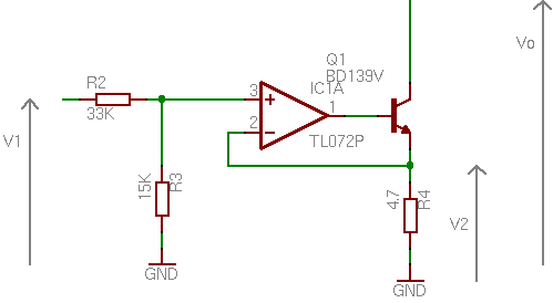
[[Image:lps_output_load_study.png|thumb|384px|left|Output Loads]] The output load is intended to create a variable resistive charge on the outputs. This charge is used to dump the output capacitors. The variable resistive charge is composed of a small power resistor and a medium power transistor that drives the current on the resistor. The operational amplifier maintains arround the resistor a voltage V2 that represents a fraction of the voltage V1 (0.3125). The input voltage V1 is in the range 0..5V and the voltage V2 is in the range 0..1.56V. | [[Image:lps_output_load_study.png|thumb|384px|left|Output Loads]] The output load is intended to create a variable resistive charge on the outputs. This charge is used to dump the output capacitors. The variable resistive charge is composed of a small power resistor and a medium power transistor that drives the current on the resistor. The operational amplifier maintains arround the resistor a voltage V2 that represents a fraction of the voltage V1 (0.3125). The input voltage V1 is in the range 0..5V and the voltage V2 is in the range 0..1.56V. | ||
| + | |||
| + | ==Schematics== | ||
| + | ===Positive Voltage Regulator=== | ||
| + | [[Image:lps_posisitive_regulator.png|thumb|384px|left|Positive Voltage Regulator]] | ||
| + | |||
| + | ===Positive Output Transistors=== | ||
| + | [[Image:lps_posisitive_outputs.png|thumb|384px|left|Positive Output Transistors]] | ||
| + | |||
| + | ==PCB== | ||
| + | ===Positive Output Transistors=== | ||
| + | [[Image:lps_posisitive_outputs_placement.png|thumb|384px|left|Positive Output PCB Placement]] The positive output transistors board contains the TO3 output transistors and the board is mounted on the heat sink. On the heat sink the TO3 transistors are rotated by 220 degree. The two NPN load transistors are also on the heat sink but not on the board. Their placement is not really good but they will not really be soldered there: cables will be used. | ||
| + | |||
| + | [[Image:lps_posisitive_outputs_bottom.png|thumb|384px|left|Positive Output PCB]] For the auto-layout the following class have been used in Eagle: | ||
| + | |||
| + | <table border="1"> | ||
| + | <tr> | ||
| + | <th>Signal class</th> | ||
| + | <th>Width</th> | ||
| + | <th>Clearance</th> | ||
| + | <th>Drill</th> | ||
| + | </tr> | ||
| + | <tr> | ||
| + | <tr> | ||
| + | <td>GND</td> | ||
| + | <td>3mm</td> | ||
| + | <td>0.5mm</td> | ||
| + | <td>1mm</td> | ||
| + | </tr> | ||
| + | <tr> | ||
| + | <td>Supply</td> | ||
| + | <td>3mm</td> | ||
| + | <td>0.5mm</td> | ||
| + | <td>1mm</td> | ||
| + | </tr> | ||
| + | <tr> | ||
| + | <td>Signal</td> | ||
| + | <td>0.6mm</td> | ||
| + | <td>0.5mm</td> | ||
| + | <td>0.6mm</td> | ||
| + | </tr> | ||
| + | <tr> | ||
| + | <td>Others</td> | ||
| + | <td>0.8mm</td> | ||
| + | <td>0.5mm</td> | ||
| + | <td>0.8mm</td> | ||
| + | </tr> | ||
| + | </table> | ||
| + | |||
| + | For the auto-routing, the clearance was set to 0.3 and 0.4mm. It was increased to 0.5mm which corresponds more or less to the maximum for this board. The GND and other polygons have been drawn at the end because the auto-router fails to route those signals if a polygon exits. | ||
Revision as of 05:38, 21 January 2007
Contents |
Description
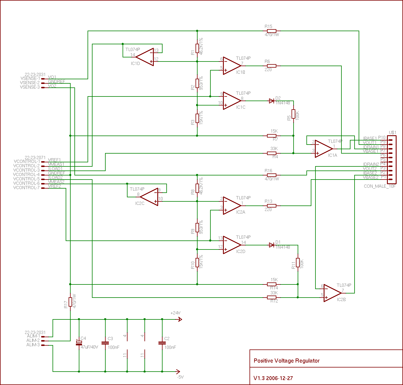
The power supply regulator is responsible for regulating the voltage of the output power supply. It is composed of two boards, one that integrates the voltage regulator for 2 power supplies and another board that contains the output power transistor and last stage filter.
Output Current Protection
The system has in fact two output current protections. One in the power supplt controller board and another one in the voltage regulator board. The first protection has an impact on the voltage reference that drives the regulator board. The second protection is more traditional. A resistor R2 combined with a switch as expained in the Rectifier board are used to measure the output current. The limiting protection consists of the two transistors Q1 and Q2. The PNP transistor Q2 is activated when the current through R2 is above the 1.3V limit. When this happens a current flows in the NPN transistor Q1 which turns it on. This draws all the current from the operational amplifier which drives the output darlington transistor Q3. The output voltage will then be reduced thus switching off Q3 and reducing the output current.
Output Load
The output load is intended to create a variable resistive charge on the outputs. This charge is used to dump the output capacitors. The variable resistive charge is composed of a small power resistor and a medium power transistor that drives the current on the resistor. The operational amplifier maintains arround the resistor a voltage V2 that represents a fraction of the voltage V1 (0.3125). The input voltage V1 is in the range 0..5V and the voltage V2 is in the range 0..1.56V.Schematics
Positive Voltage Regulator
Positive Output Transistors
PCB
Positive Output Transistors
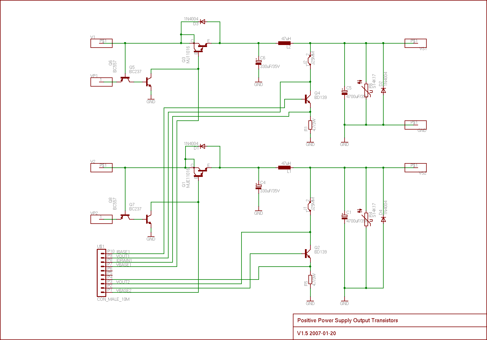
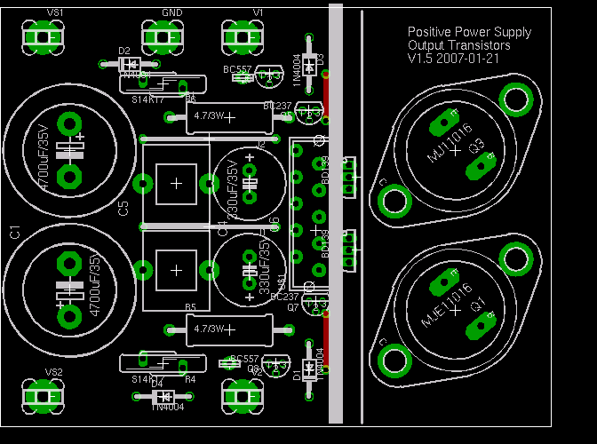
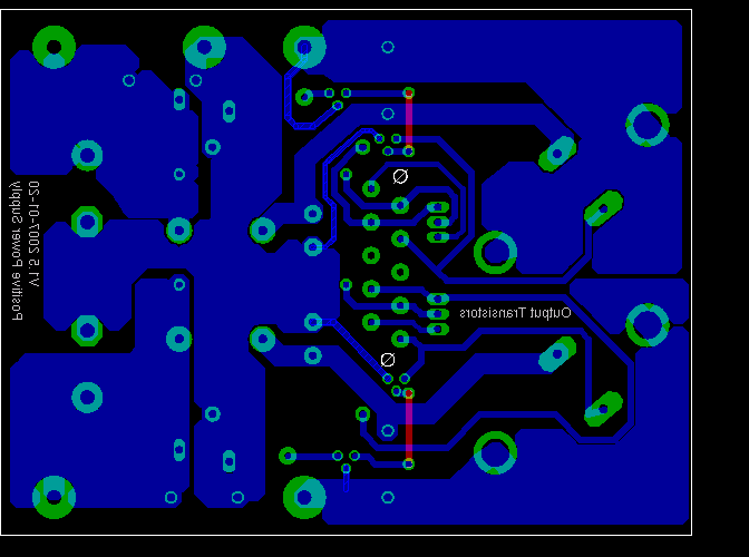
The positive output transistors board contains the TO3 output transistors and the board is mounted on the heat sink. On the heat sink the TO3 transistors are rotated by 220 degree. The two NPN load transistors are also on the heat sink but not on the board. Their placement is not really good but they will not really be soldered there: cables will be used. For the auto-layout the following class have been used in Eagle:| Signal class | Width | Clearance | Drill |
|---|---|---|---|
| GND | 3mm | 0.5mm | 1mm |
| Supply | 3mm | 0.5mm | 1mm |
| Signal | 0.6mm | 0.5mm | 0.6mm |
| Others | 0.8mm | 0.5mm | 0.8mm |
For the auto-routing, the clearance was set to 0.3 and 0.4mm. It was increased to 0.5mm which corresponds more or less to the maximum for this board. The GND and other polygons have been drawn at the end because the auto-router fails to route those signals if a polygon exits.
