VACS:Projects:Hardware:LPS:RegulatorBoard
(→Connectors) |
|||
| Line 42: | Line 42: | ||
<td>IBASE2</td> | <td>IBASE2</td> | ||
<td></td> | <td></td> | ||
| − | <td>Load current transistor base driver | + | <td>Load current transistor base driver</td> |
</tr> | </tr> | ||
<tr> | <tr> | ||
| Line 72: | Line 72: | ||
<td>VBASE1</td> | <td>VBASE1</td> | ||
<td></td> | <td></td> | ||
| − | <td></td> | + | <td>Output transistor base driver</td> |
<td rowspan="4">Power supply 1</td> | <td rowspan="4">Power supply 1</td> | ||
</tr> | </tr> | ||
| Line 79: | Line 79: | ||
<td>IDRAIN1</td> | <td>IDRAIN1</td> | ||
<td></td> | <td></td> | ||
| − | <td> | + | <td>Load drain feedback</td> |
</tr> | </tr> | ||
<tr> | <tr> | ||
| Line 85: | Line 85: | ||
<td>VOUT1</td> | <td>VOUT1</td> | ||
<td></td> | <td></td> | ||
| − | <td> | + | <td>Output voltage sense</td> |
</tr> | </tr> | ||
<tr> | <tr> | ||
| Line 91: | Line 91: | ||
<td>IBASE1</td> | <td>IBASE1</td> | ||
<td></td> | <td></td> | ||
| − | <td> | + | <td>Load current transistor base driver</td> |
</tr> | </tr> | ||
</table> | </table> | ||
Revision as of 09:07, 7 May 2007
| Status | |
|---|---|
| Schema finished | |
| Validated the schema | |
| Validated the board layout | |
| Board manufactured | |
| Board finished | |
| Board tested | |
Contents |
Description
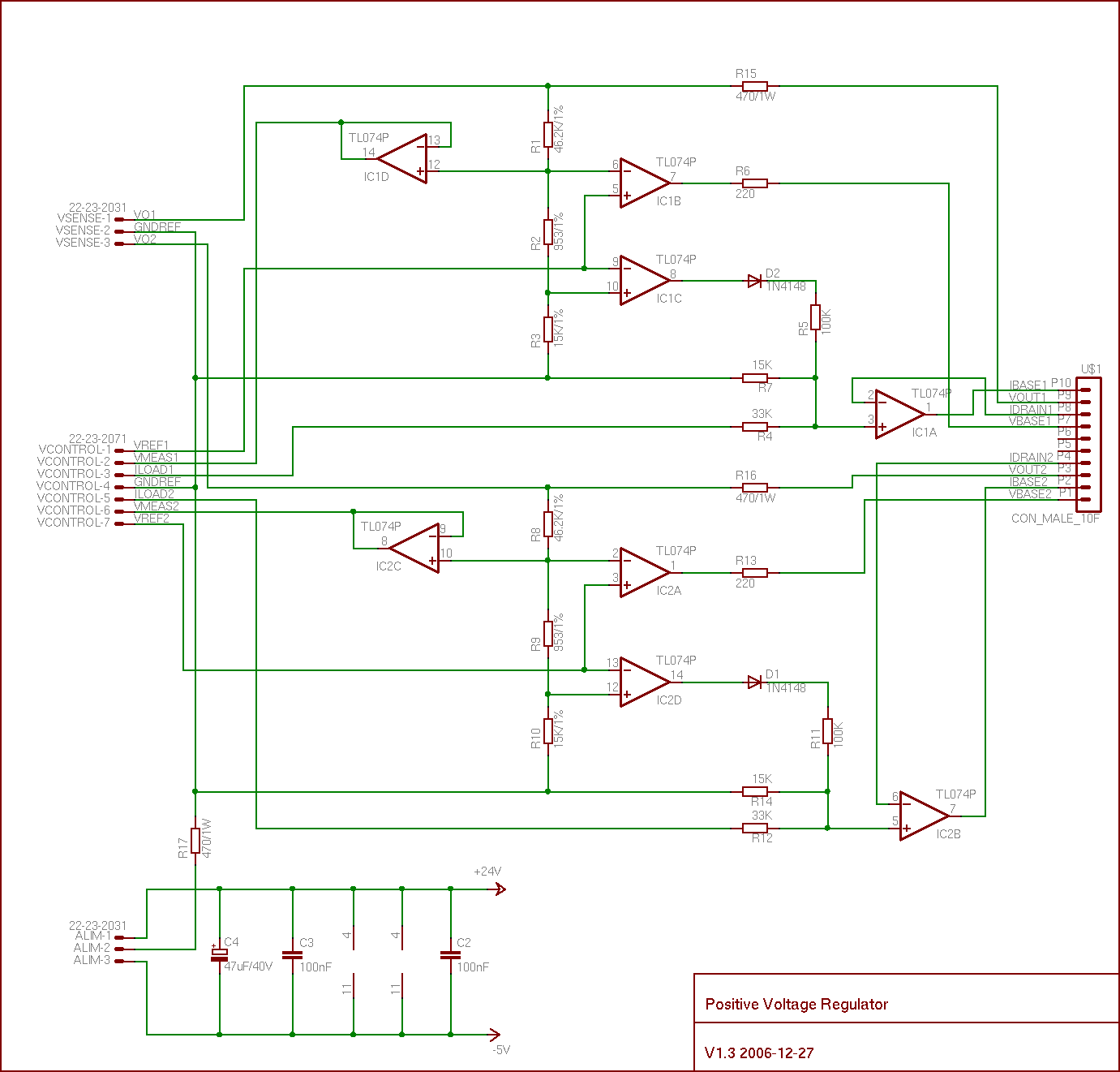
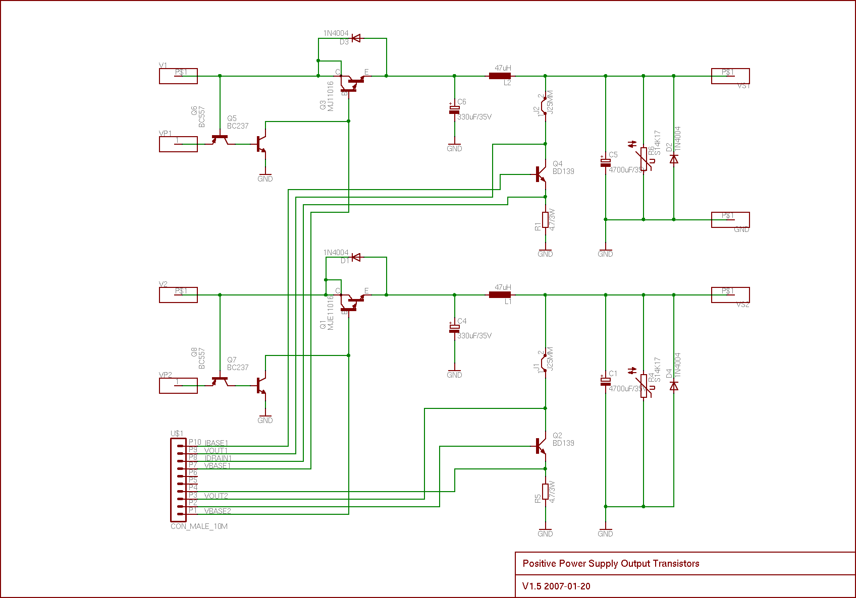
The power supply regulator is responsible for regulating the voltage of the output power supply. It is composed of two boards, one that integrates the voltage regulator for 2 power supplies and another board that contains the output power transistor and last stage filter.
Output Current Protection
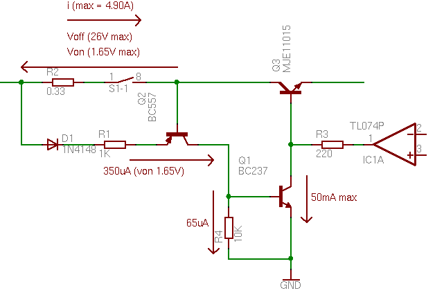
The system has in fact two output current protections. One in the power supplt controller board and another one in the voltage regulator board. The first protection has an impact on the voltage reference that drives the regulator board. The second protection is more traditional. A resistor R2 combined with a switch as expained in the Rectifier board are used to measure the output current. The limiting protection consists of the two transistors Q1 and Q2. The PNP transistor Q2 is activated when the current through R2 is above the 1.3V limit. When this happens a current flows in the NPN transistor Q1 which turns it on. This draws all the current from the operational amplifier which drives the output darlington transistor Q3. The output voltage will then be reduced thus switching off Q3 and reducing the output current.
Output Load
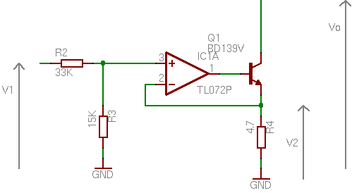
The output load is intended to create a variable resistive charge on the outputs. This charge is used to dump the output capacitors. The variable resistive charge is composed of a small power resistor and a medium power transistor that drives the current on the resistor. The operational amplifier maintains arround the resistor a voltage V2 that represents a fraction of the voltage V1 (0.3125). The input voltage V1 is in the range 0..5V and the voltage V2 is in the range 0..1.56V.
Schematics
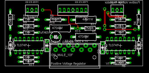
Positive Voltage Regulator
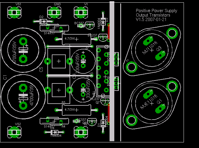
Positive Output Transistors
Connectors
The rectifier board is connected to the power supply microcontroller board for the control and measurement of the output current. For the power distribution it has several one wire high power connectors (not described here). The positive and negative power supply rectifier boards have the same connector.
| POWER_CONTROL | ||||
|---|---|---|---|---|
| 1 | VBASE2 | Output transistor base driver | Power supply 2 | |
| 2 | IBASE2 | Load current transistor base driver | ||
| 3 | VOUT2 | Output voltage sense | ||
| 4 | IDRAIN2 | Load drain feedback | ||
| 5 | GND | |||
| 6 | GND | |||
| 7 | VBASE1 | Output transistor base driver | Power supply 1 | |
| 8 | IDRAIN1 | Load drain feedback | ||
| 9 | VOUT1 | Output voltage sense | ||
| 10 | IBASE1 | Load current transistor base driver | ||
PCB
Positive Output Transistors
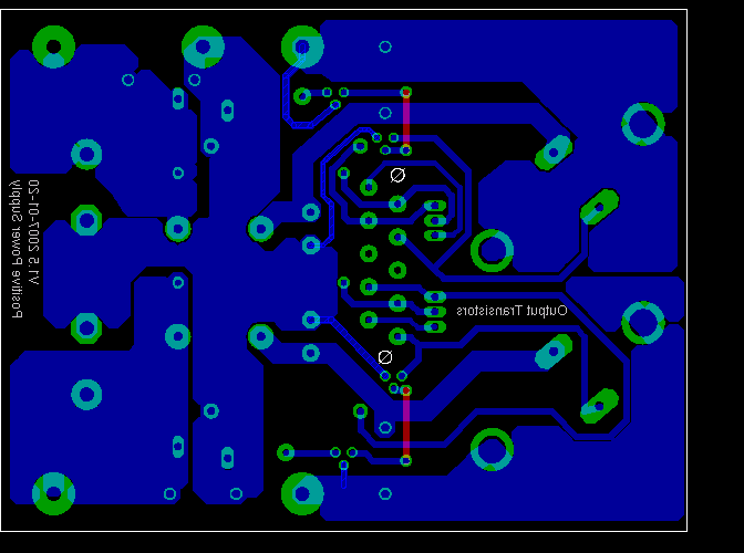
The positive output transistors board is Xmm x Ymm wide with a 70um copper side. It contains the TO3 output transistors and the board is mounted on the heat sink. On the heat sink the TO3 transistors are rotated by 220 degree. The two NPN load transistors are also on the heat sink but not on the board. Their placement is not really good but they will not really be soldered there: cables will be used.
| Signal class | Width | Clearance | Drill |
|---|---|---|---|
| GND | 3mm | 0.5mm | 1mm |
| Supply | 3mm | 0.5mm | 1mm |
| Signal | 0.6mm | 0.5mm | 0.6mm |
| Others | 0.8mm | 0.5mm | 0.8mm |
For the auto-routing, the clearance was set to 0.3 and 0.4mm. It was increased to 0.5mm which corresponds more or less to the maximum for this board. The GND and other polygons have been drawn at the end because the auto-router fails to route those signals if a polygon exits.
Positive Regulator
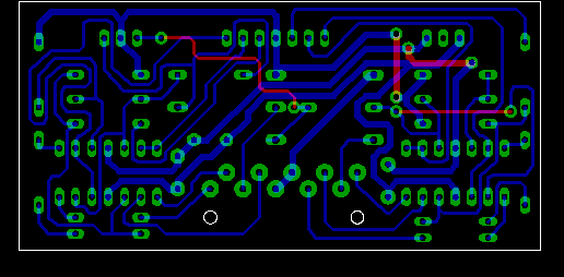
The positive regulator placement board is 81mm x 39mm wide on a single sided 35um board. The connector is used to plug it on the positive output transistor board.
| Signal class | Width | Clearance | Drill |
|---|---|---|---|
| Supply | 0.8mm | 0.4mm | 0.8mm |
| Signal and others | 0.4mm | 0.4mm | 0.8mm |
Datasheets
Below is a collection of datasheets, white papers and articles related to the parts used in the board.
Resistors
Capacitors
- [SOLID POLYMER ALUMINUM CAPACITOR CHIPS IN DC-DC CONVERTER MODULES REDUCE COST AND SIZE AND IMPROVE HIGH-FREQUENCY PERFORMANCE ]
- [CONDUCTIVE POLYMER ALUMINUM SOLID ELECTROLYTIC CAPACITORS ]
- [Electrolytic Capacitor Guide ]
- [EPCOS Electrolytic Aluminium Capacitor (4700uF/40V) ]
Semiconductors
- [TL074 operational amplifiers ]
- [BC237 NPN Epitaxial Transistor ]
- [BC557 PNP Epitaxial Transistor ]
- [BD139 NPN Transistor ]
- [BD140 PNP Transistor ]
- [MJ11015.pdf PNP Silicon Darlington Transistor ]
- [MJ11016.pdf NPN Silicon Darlington Transistor ]
